
Insert molding services are a key support for the manufacturing of core components in semiconductor equipment.
With precise process control, semiconductor insert molding can efficiently address sealing failures at micron levels and ion contamination issues, thus stopping the waste of entire batches of wafers worth millions of dollars.
The insert molding technology provided by JS Precision combines metal strength with the stability of special plastics, ensuring that components achieve a vacuum degree of 10 ⁻⁹ mbar/l. s, reducing wafer defect rates, and redefining the reliability standards for semiconductor components.
When semiconductor equipment is pushed to higher vacuum levels and more corrosive environments, traditional mechanical assembly will no longer be able to fulfill the needs, insert molding has become the main process for solving bottlenecks.
Core Answer Summary
|
Core Dimension
|
Key Technical Solutions
|
Business Value
|
Core Data
|
|
Contamination Control
|
Class 100 Cleanroom Production + 18MΩ·cm Deionized Water Ultrasonic Cleaning
|
Reduce Wafer Defect Rate.
|
Wafer defect rate is reduced by more than 30%.
|
|
Material Sealing
|
Chemical Bonding Process of PEEK/PFA and Metal
|
Ensure High Vacuum Level.
|
Stably reach a vacuum level of 10⁻⁹ mbar/l.s.
|
|
Precision Standard
|
Automatic Manipulator Positioning + ±0.01mm Tolerance Control
|
Extend Equipment Mean Time Between Failures.
|
MTBF is extended to more than 8000 hours.
|
|
Thermal Expansion Matching
|
30% Carbon Fiber Filled Polymer + 150°C Insert Preheating
|
Avoid Interface Delamination.
|
Interface delamination rate is reduced to below 0.1%.
|
|
Production Efficiency
|
Integrated Molding + Automatic Demolding
|
Shorten Supply Chain Lead Time.
|
Lead time is shortened by 30%, and assembly cycle is shortened by 40%.
|
Key Takeaways
- Airtightness Guarantee: Fully encapsulate the insert to remove the possibility of vacuum leakage indicating totally eliminate the vacuum leakage point caused by mechanical joint gap.
- Design Priority: Careful consideration of wall thickness and proper use of ribs according to established guidelines will be the key factors in avoiding cracking after molding.
- Material Matching: Using advanced polymeric materials whose coefficients of thermal expansion are very close to those of metals help in preventing interfacial delamination.
- One Stop Delivery: JS Precision not only does the processing but also the injection molding which results in reduced supply chain lead time by 30%.
Why Choose JS Precision’s Insert Molding Services? Semiconductor Precision Manufacturing Solutions
Insert molding is a fundamental manufacturing process for your semiconductor equipment components. Selecting a reliable insert molding services provider is extremely important to minimizing production risks while also expanding production capacity.
As a semiconductor company, you want the provider who can really understand your requirements and give you value at the same time. JS Precision is a good example.
By procuring our top class services, which strictly meet the ISO 14644-1 semiconductor cleanroom standard, you can acquire components solutions that conform to a global level.
Choosing JS Precision will give you a Class 100 cleanroom production environment plus 18MΩ·cm deionized water ultrasonic cleaning technology.Thus, the wafer defect rates are directly decreased by over 30%, which will allow you to avoid losses from wafer scrap.
Our automated robotic positioning and 0.01mm tolerance control technology will help you to ramp up the mean time between failures (MTBF) to over 8000 hours, thereby decreasing downtime related capacity losses and cost waste.
Another international semiconductor customer, who had the same equipment needs, had to face wafer scrap losses due to component seal failures amounting to over $500,000 every year.
You can refer to their results after deciding to use our insert molding services as a result, not only they kept the leakage rate stable at 10⁻⁹ mbar/l.s, but they also managed to raise the component yield rate from 65% to 99.2%, thereby saving over $400,000 every year.
Moreover, you can make use of our team's well rooted DFM engineering experience to get expert professional optimization advice from the design step, which can help shorten supply chain lead times by 30%, improve your product launch time, and seize market opportunities readily.
JS Precision puts your needs first, combines mold design, material selection, and manufacturing services all through the process.
Thus, there will be no need for you to find multiple suppliers, which in turn minimizes communication costs, supply chain risks, and also makes component production more worry free and efficient.
If you are struggling with component sealing, precision control, or other issues, contact our engineering experts immediately for personalized semiconductor insert molding technical consultation.
Why Is Precision Insert Molding For Semiconductor Equipment Essential?
The extremely harsh operating conditions of semiconductor machines require components to be extremely airtight and clean. As a central procedure, insert molding effectively addresses the disadvantages of traditional assembly methods.
Semiconductor insert molding involves directly molding high performance plastics onto metal backings, thereby removing the need for fasteners and seals.
This not only ensures excellent physical isolation performance in extreme environments, but it is also the main factor for enhancing component integration and airtightness.
Improving Structural Strength in Ultra High Vacuum Conditions
Conventional mechanical seals are a source of wafer contamination in 10⁻⁷ Torr environments due to micro gap gas leakages. Insert molding fabricates an uninterrupted physical barrier that makes gas permeation impossible.
To put it simply, a seamless protective suit is wrapped around the component, making the leakage completely impossible.
Integration of benefits:
- Mechanical gaps, which are the origin of gas infiltration and particle generation, are eliminated, thereby maintaining wafer cleanliness.
- The intrinsic strength of metals is combined with the dimensional stability of plastics, which is a key factor in increasing component lifespan and decreasing replacement costs.
Getting Rid of Secondary Assembly Risks and Particle Sources
Thermal expansion and contraction cause mechanical fastener vibration and micro debris generation, which can directly make a wafer unusable.
Insert molding mainly takes 5-10 parts and turns them into one single integral component, which means that debris is eliminated at its very source, and assembly steps are greatly reduced.It can shorten assembly cycles by more than 40%, reduce BOM costs by 20%-30%, and reduce human error.
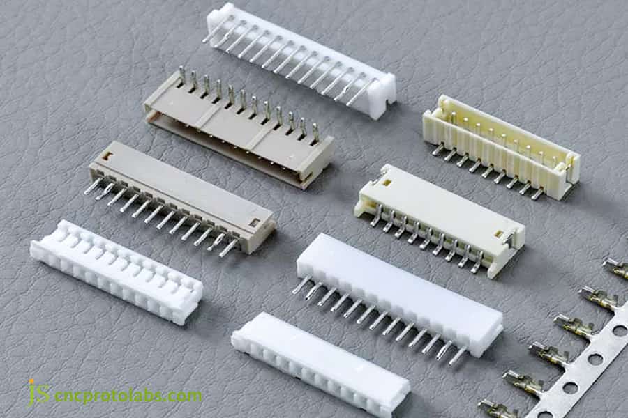
Figure 1: A display of various white and beige precision pin connectors with metal inserts, showcasing the outcome of insert molding for semiconductor applications.
What Are The Critical Rules In a Semiconductor Insert Molding Design Guide?
Proper design is the first step toward ensuring a successful insert molding.
The main focus of insert molding design guide is on controlling plastic wall thickness, creating mechanical interlocking structures, and allocating insert support positions to give the component the ability to keep its shape and strength when subjected to high pressure.
Simply put, this is like making a house - you need to have a good foundation and a strong frame. By following the basic rules, you can prevent problems such as cracking and loosening from occurring later, thus guaranteeing the components' stable function over time.
Wall Thickness Consistency and Gate Location Optimization
Semiconductor components require that the wall thickness be kept constant at 1.5-3.0mm, if not, the areas of tensile stress will concentrate and result in cracking, equally to how a wall that is not uniformly thick can lead to cracking. Uniform wall thickness leads to uniform stress distribution.
We employ Moldflow simulation to identify the position of weld lines to make sure that they do not locate the critical high pressure, high vacuum sealing areas that can be the cause of seal failure.
Mechanical Interlocking Features for Metal Plastic Bonding
Metal plastic bond strength is improved by geometric interlocking. We implement metal inserts with undercuts (0.2mm), knurling (0.5-1.0mm pitch), or through holes (1.0mm).
For small sensor pins, we design a non circular symmetrical fixing structure to prevent loosening of the wiring later on, ensuring component stability.
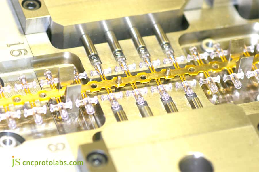
Figure 2: A detailed view of metallic inserts precisely positioned within a golden-colored mold base, highlighting the tooling for semiconductor component manufacturing.
Which Metal Insert Molding Solutions Solve Thermal Expansion Mismatch?
Differences in the coefficient of thermal expansion (CTE) are one of the main problems in metal insert molding that may cause component delamination and seal failure. Use of preheating the insert, filler fiber polymers and buffer zones are the most effective methods.
Thermal Expansion Coefficient (CTE) Matching Strategies
Differences in CTE between different materials affect component stability. CTE data for commonly used materials are as follows:
|
Material Type
|
Material Specification
|
CTE at 25°C (ppm/°C)
|
CTE at 100°C (ppm/°C)
|
CTE at 180°C (ppm/°C)
|
Application Scenario
|
|
Metal Insert
|
Stainless Steel 316L
|
16
|
17.2
|
18.5
|
High Vacuum Sealing Components
|
|
Metal Insert
|
Aluminum Alloy 6061
|
23.1
|
24.5
|
26.3
|
Lightweight Components
|
|
Metal Insert
|
Kovar Alloy
|
5.9
|
6.1
|
6.3
|
High Precision Sensor Components
|
|
Plastic Material
|
Pure PEEK
|
50
|
58
|
65
|
Conventional Corrosion-Resistant Components
|
|
Plastic Material
|
30% Carbon Fiber PEEK
|
18
|
20
|
22
|
Thermal Expansion Matching Components
|
|
Plastic Material
|
PFA
|
70
|
78
|
85
|
Plasma-Resistant Components
|
Preheating Processes and Controlled Cooling Cycles
We make use of a programmable temperature controller in order to perform staged cooling which results in the prevention of uneven molecular chain crystallization caused by rapid cooling and ensures that the module stays dimensionally stable.
Facing thermal expansion mismatch challenges? Contact our engineering experts for free customized insert molding solutions and CTE matching solutions to resolve interface delamination issues.
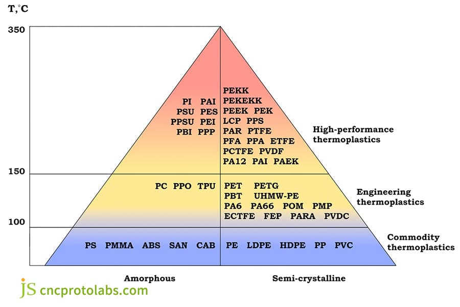
Figure 3: A triangular pyramid diagram categorizing various thermoplastics, from commodity to high-performance, based on their temperature resistance and crystallinity.
How To Select Materials For High-Performance Custom Insert Molding?
The materials you select for custom insert molding will set the performance of your module and should be matched with the processing application:
For plasma resistant PFA/PEEK in etching equipment, for low outgassing materials to photolithography equipment, check always the conformity with the IEC 61709 semiconductor device reliability standards as well as the purity and dielectric constant requirements.
In other words, different semiconductor equipment operating conditions, like different working environments, require different clothes to be worn.
Choosing the right materials can make the components "wear-resistant and durable" in complex environments, avoiding equipment failures and wafer scrap caused by unsuitable materials.
Performance Polymers for Corrosive Chemical Resistance
PFA and PTFE are very stable in strong acidic environments such as the hydrofluoric acid and show no corrosion or deformation, they also maintain their sealing performance even after prolonged exposure.
Expert insert molding can accurately synchronize these corrosion resistant materials and help you use their features to their fullest extent.
Structural strength is one of the advantages of PEEK (Young's modulus 3.8 GPa) over PPS (2.6 GPa). We shall advise on the materials that best fit the strength requirements.
Low Outgassing Requirements for Ultra High Vacuum
Material total mass loss (TML) must be 0.1% in semiconductor applications, otherwise, the released volatiles will contaminate the wafer, causing it to be scrapped.
How Do Modern Insert Molding Services Minimize Particle Contamination?
The particle contamination level allowed in semiconductor components is extremely low. Professional insert molding services achieve this through cleanroom operations, management of high purity raw materials, and automated demolding.
These measures can control particle contamination to semiconductor grade levels, thus guaranteeing that the wafer will not be contaminated by the component.
Implementing Cleanroom Manufacturing Standards (Class 100/1000)
JS Precision ensures air quality in the injection molding area through a HEPA filtration system. The particle control standards for different cleanrooms are as follows:
|
Cleanroom Class
|
Number of Particles ≥0.5μm per Cubic Foot
|
Number of Particles ≥5μm per Cubic Foot
|
Applicable Process Stages
|
Customer Benefits
|
|
Class 100
|
≤100
|
≤0
|
Insert Molding Production, Component Cleaning.
|
Avoid particle contamination and increase component yield to over 99%.
|
|
Class 1000
|
≤1000
|
≤10
|
Raw Material Storage, Component Packaging.
|
Reduce the risk of secondary contamination during storage.
|
|
Class 10000
|
≤10000
|
≤100
|
Mold Preprocessing, Equipment Maintenance.
|
Control production costs while meeting cleanliness requirements.
|
We have very strict operating procedures. Employees are required to change into complete cleanroom suits. When entering and leaving the cleanroom, passing through an airlock for dust removal is necessary in order to prevent secondary contamination.
Leading Edge Post Molding Deionization and Cleaning Operations
To ultrasonic clean of the component surfaces to remove residual micro dust, we use 18 Ω·cm deionized water, which ensures the surfaces have a cleanliness level corresponding to semiconductor standards.
Then cleaning, the packaging with double layer vacuum aluminum foil is done straight in the cleanroom so that no particle adsorption occurs during transportation.
Want to learn how Class 100 cleanroom insert molding services control particulate contamination? View our success stories for detailed technical information.
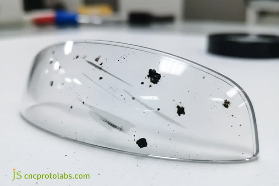
Figure 4: A close-up of a transparent molded component with black particulate contamination on its surface, highlighting a quality control concern.
What Makes a Trusted Custom Insert Molding Manufacturer For The Chip Industry?
As semiconductor companies aim for component accuracy and risk reduction in their supply chains, they cannot afford to leave the trust in their custom insert molding manufacturer up to chance.
A company capable of producing a semiconductor grade quality management system, using precise test equipment, and with a great deal of experience in DFM (Design for Manufacturing) is the most likely to be successful.
Precision Metrology and 0.01mm Tolerance Control
We conduct full precision testing, monitoring insert positioning with a CCD image measurement system in real time (accuracy 0.005mm). Continuing cross sectional analysis of interface filling quality helps us ensure no voids or air bubbles are present.
We have a complete quality traceability system in place. Detailed testing records of each batch of products are available for the traceability of raw materials, parameters, and results, guaranteeing the product's compliance.
Vertical Integration from Mold Design to Mass Production at JS Precision
Being equipped with an in house mold workshop, we have achieved vertical integration from mold design and manufacturing to insert molding production and testing. By doing so, the DFM feedback cycle is reduced to 24 hours, allowing us to respond quickly to design changes.
What Are The Top Challenges And Solutions In Semiconductor Insert Molding?
Semiconductor insert molding is a process that requires precision at a very high level. The major issues faced include insert displacement, reduced weld line strength, and hermeticity failure.
Compliance with the ISO 13485 semiconductor component quality management standard can help in reducing the risks, and these issues can be thoroughly tackled by using accurate technologies.
Preventing Insert Displacement Under High Injection Pressure
The high pressure of injecting 800-1500 bars can cause insert displacement very easily (displacement more than 0.02 mm is the condition of failure). The well developed insert molding solutions can totally prevent this problem. The particular remedies are:
- Hydraulic assisted locking + precision locating pins that can guarantee that even the inserts with high aspect ratio will have a displacement of less than 0.02 mm.
- Multistage pressure control facilitates the injection of an optimal curve, and the filling of the low velocity at the beginning safeguards the precision pins.
Enhancing Interfacial Bonding Strength via Plasma Treatment
Weak bonding of metal and plastic interfaces is a reason for delamination and seal failure. The first way to strengthen the bond is:
Treatment with atmospheric plasma that removes organic matter and oxide layers from the metal surface, achieves molecular level bonding, and increases the peel strength by more than 50%.
Use of specialized coupling agents in order to enhance the bonding of metals and plastics that are specific to each other and prevent the parts from coming apart even after long term thermal cycling.
JS Precision Case Study: Precision Packaging Of High Vacuum Chamber Sensor Components
Insert molding services play a vital role in the production of high vacuum sensor parts. By addressing sealing issues for sensor components, we have not only improved sealing performance but also ensured precision in detection and high quality of wafers for semiconductor customers.
Problems faced:
The sensor component made by the customer includes five 0.8mm stainless steel 316L pins embedded in a PEEK housing, and the leakage rate needs to be 10⁻⁴ mbar/l·s.
After cycling at high and low temperatures from 20℃ to 180℃, traditional processes are resulting in interface delamination due to the large difference in CTE (chemical ester residue).
Due to this, the leak rate is 10⁻⁴ mbar/l·s, production yield is only 65%, and mass production is not possible, all of which have caused mold and raw material losses, and market launch delays.
Solution:
We came up with a simple three step plan to fix the problems you mentioned, which also bring together metal insert molding technology to accurately solve the issues of interface delamination and seal failure.
This is a typical example of metal insert molding in high vacuum component encapsulation:
1. In order to reduce the temperature difference between stainless steel pins and the PEEK melt, minimize the internal stress caused by thermal shock, and prevent shrinkage cracking after plastic molding, a preheating circulation system was introduced to preheat the stainless steel pins to 150℃.
2. Based on the principle that increasing surface area can lead to stronger bonding, nanoscale laser micro etching was done on the pin surface, which increased the surface area by 40%, thereby improving the mechanical interlocking force between the plastic and metal, and enhancing the strength of the interface bond.
3. The injection pressure was accurately set at 1200 bar and the holding time was lengthened to 30 seconds to guarantee that the plastic completely fills the mold gaps, and a 4-hour post annealing step was incorporated to help release residual stress and make the component dimensions more stable.
Lessons Learned from Failure:
The first batch of finished products was fine for immediate use however after 48 hours microcracks surfaced as the result of stress release and the leakage rate increased again.
This taught us that we should have a programmable mold temperature controller to cool the mold gradually in stages so that the residual stress can be fully released.
A regular ultrasonic cleaning will not be able to get rid of the oil and dirt in the micropores of the pins. Cleaning with atmospheric plasma is necessary for the detachment of oil and dirt, it alters surface energy and the bonding comes down to molecular level.
Final Results:
The finished product was qualified in passing 100 high and low temperature shock tests, and helium mass spectrometry leak detection had a stable reading of 10 mbar/ls.
Production increase from 65% to 99.2%, opening the door to mass production, the customer's monthly loss was reduced by the amount of $80,000, and time-to-market was accelerated.
If you also face challenges such as sensor component sealing and interface delamination, contact our engineering experts for a customized metal insert molding solution.
FAQs
Q1: What vacuum level can insert molding achieve?
With the introduction of optimal interface bonding process, insert molding can keep helium leakage detection at a level of 10⁻⁹ mbar/l·s, which is in line with the standard of semiconductor high vacuum equipment and also eliminates the leakage of gas that leads to wafer contamination.
Q2: What materials are typically used for metal inserts?
Semiconductor insert molding normally uses metal materials like 316L stainless steel, 6061 aluminum alloy, and Kovar alloy. We will suggest the most appropriate material after careful consideration of the component's use and working environment.
Q3: How to prevent insert displacement during injection molding?
Inserts displacement is minimized to 0.01mm level via precision positioning pins and automated vision checking. Besides, by manufacturing the injection cycle based on this data to avoid high pressure deviation, accuracy of the dimensions is guaranteed.
Q4: What is the maximum temperature resistance of the component?
By making use of special plastics like PEEK, the component can easily work at 250℃ for a long time and can tolerate a short period of temperature as high as 300°C. This satisfies the temperature specifications of semiconductor equipment.
Q5: How to enhance the bonding strength between metal and plastic?
The bonding strength will be greatly improved if laser micro etching, plasma cleaning, and mechanical interlocking design are all combined. They also effectively avoid interface delamination.
Q6: What is the minimum supported insert size?
JS Precision is capable of processing precision lead inserts with a diameter of 0.5mm, which can position precisely and mold stably the semiconductor micro components.
Q7: Can you provide DFM design support?
We can offer you various insert molding design guide consultation and Moldflow simulation for the optimization of your designs, defect avoidance, cost reduction, and efficiency improvement.
Q8: What is the typical prototyping cycle before mass production?
The precision mold and first sample development for semiconductor insert molding products usually takes 4 to 6 weeks. We will make every effort to shorten the time to market for our customers through process acceleration.
Summary
Precision and reliability in semiconductor equipment are tightly linked to expert semiconductor insert molding technology. Each micron level accuracy and every seal stability are directly related to wafer quality and enterprise costs.
Mature insert molding solutions from JS Precision is like a magic wand to tackle the core problems such as component sealing precision thermal expansion matching, etc. that help in cost reduction, yield improvement, and short delivery time.
A stable and efficient insert molding service is what you get when you choose us, making your core component a competitive advantage for your equipment. To improve components and optimize the process, get in touch with our engineering experts now for the best solutions and quotes.

Disclaimer
The contents of this page are for informational purposes only.JS Precision Services,there are no representations or warranties, express or implied, as to the accuracy, completeness or validity of the information. It should not be inferred that a third-party supplier or manufacturer will provide performance parameters, geometric tolerances, specific design characteristics, material quality and type or workmanship through the JS Precision Network. It's the buyer's responsibility Require parts quotation Identify specific requirements for these sections.Please contact us for more information.
JS Precision Team
JS Precision is an industry-leading company, focus on custom manufacturing solutions. We have over 20 years of experience with over 5,000 customers, and we focus on high precisionCNC machining,Sheet metal manufacturing,3D printing,Injection molding,Metal stamping,and other one-stop manufacturing services.
Our factory is equipped with over 100 state-of-the-art 5-axis machining centers, ISO 9001:2015 certified. We provide fast, efficient and high-quality manufacturing solutions to customers in more than 150 countries around the world. Whether it is small volume production or large-scale customization, we can meet your needs with the fastest delivery within 24 hours. Choose JS Precision this means selection efficiency, quality and professionalism.
To learn more, visit our website:www.cncprotolabs.com
Resource