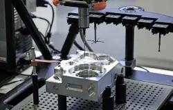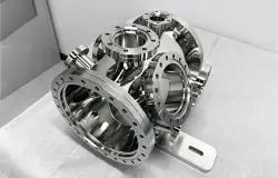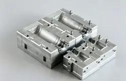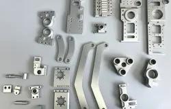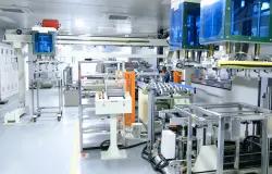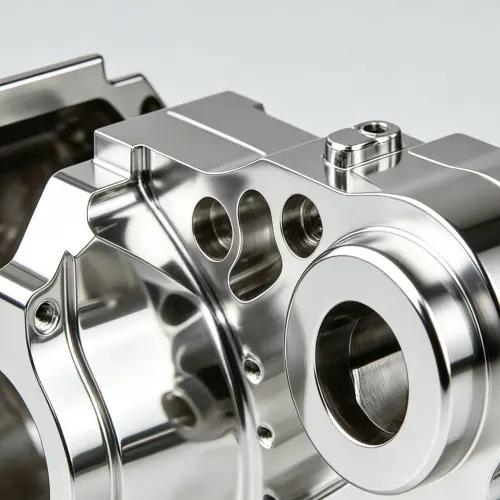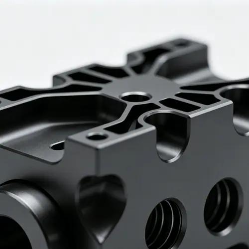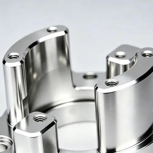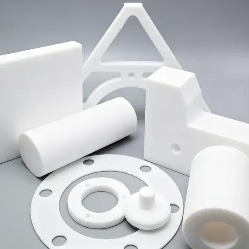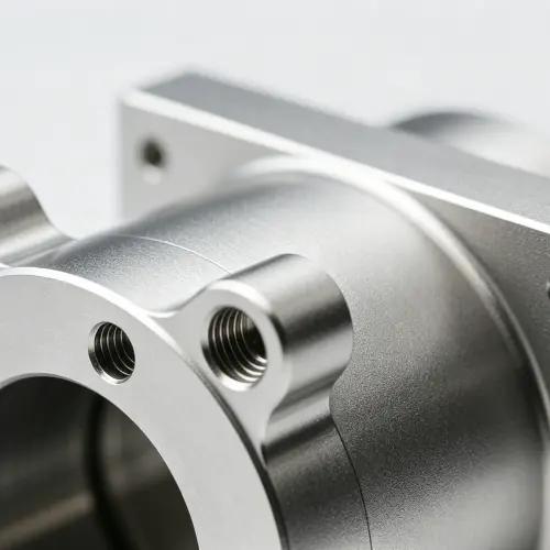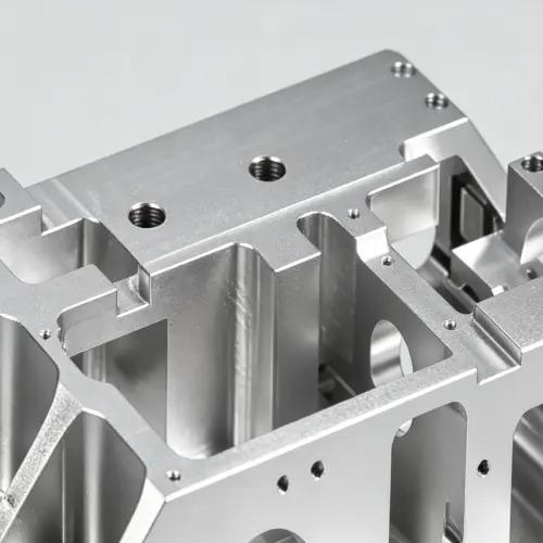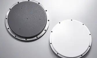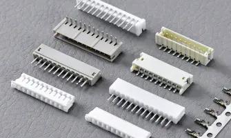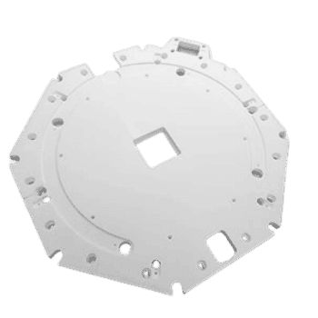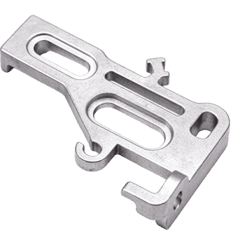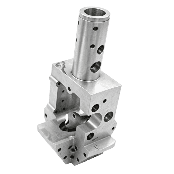








High precision semiconductor fabrication for reliable industrial production

Industries / Semiconductor

High Precision Semiconductor Fabrication for Reliable Industrial Production

Expert manufacturing solutions deliver standardized high performance components that ensure process consistency across diverse semiconductor production environments.

View Custom Solutions

Certification + Compliance

ISO 9001:2015 | Cleanroom Class 100/1000 | RoHS & REACH | SEMI S2/S8 | AS9100D

Trusted by GlobalSemiconductor Leaders

Advantest logo
MKS Instruments logo
Tokyo Electron logo
Entegris logo
VAT Valve logo
Semiconductor partner logo
Advantest logo
MKS Instruments logo
Tokyo Electron logo
Entegris logo
VAT Valve logo
Semiconductor partner logo

2000+ Happy Customers

ISO 9001

2015 certification

Why Choose JS Precision as Your Manufacturing Partner

Professional manufacturing services resolve core challenges in semiconductor hardware through comprehensive engineering solutions.

icon

Accelerated Production Cycles

Optimized workflows and proactive supply chain management reduce manufacturing lead times for critical wafer processing components.

icon

Sub-Micron Precision Control

Advanced CMM verification and metrology systems ensure that all machined parts achieve the rigorous tolerances required for lithography equipment.

icon

Specialized Material Expertise

Engineering support includes high purity ceramics, fluoropolymers, and refractory metals designed to withstand aggressive chemical etching environments.

98.9%

Customer Satisfaction Rate

700+

Successful Semiconductor Projects

15+

Years of Industry Experience

98%

On-Time Delivery Performance

Comprehensive Production Support Team

A specialized manufacturing team operates behind the scenes to fulfill production requirements by managing the entire lifecycle and providing real time project updates.

Technical account liaison for semiconductor manufacturing

Technical Account Liaison

Strategic partners facilitate seamless communication by managing engineering specifications and coordinating secure digital asset transfers.

Design for manufacturability support for semiconductor hardware

Design for Manufacturability (DFM)

Specialized engineers provide advanced modeling insights and material efficiency analysis to enhance the performance of intricate hardware.

Supply chain management for semiconductor components

Supply Chain Management

Logistics professionals orchestrate precision distribution networks and lead time optimization to maintain consistent production uptime.

Metrology and verification for semiconductor fabrication

Metrology & Verification

Precision inspection specialists utilize high resolution equipment to validate dimensional accuracy against rigorous semiconductor industry standards.

How to Optimize Semiconductor Industries Precision Machining Services?

Professional manufacturing services provide critical vacuum components and chamber hardware to ensure consistent thin film deposition and etching results.

Precision CNC machined semiconductor component

Precision CNC Machining

Advanced multi axis milling delivers sub micron tolerances for critical wafer handling components and automated processing equipment.

Learn More
Injection molding and tooling for semiconductor equipment

Injection Molding & Tooling

High performance polymer molding supports the production of chemically resistant fluid handling components for specialized wet process applications.

Learn More
Rapid prototyping services for semiconductor hardware

Rapid Prototyping Services

Accelerated development cycles support fast iteration of specialized hardware to reduce time to market for new semiconductor equipment designs.

Learn More
Certified surface finishing for semiconductor components

Certified Surface Finishing

Integrated cleanroom post processing and specialized cleaning protocols prevent particulate contamination of sensitive manufacturing tools.

Learn More

High Performance Materials for Semiconductor Fabrication

Advanced material integration delivers high purity solutions for critical hardware demanding extreme thermal stability and chemical resistance.

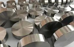
Refractory metals and superalloys for semiconductor fabrication

Refractory Metals & Superalloys

Specialized alloys like Inconel ensure durability and corrosion resistance for high temperature deposition and vacuum chamber environments.

High grade aluminum alloy semiconductor component

High Grade Aluminum Alloys

Precision machined 6061 and 7075 series aluminum offer superior electrical conductivity and stability for complex wafer handling systems.

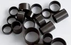
Engineering thermoplastics for semiconductor equipment

Engineering Thermoplastics

High purity polymers like PEEK and Ultem provide essential insulation and chemical resistance for specialized wet process applications.

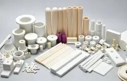
Advanced technical ceramics for semiconductor fabrication

Advanced Technical Ceramics

Alumina and Silicon Carbide components maintain critical dimensional accuracy and wear resistance within abrasive plasma processing chambers.

What are High Performance Surface Finishes for Semiconductor Fabrication?

Specialized surface treatments ensure component purity and protect critical hardware against aggressive plasma erosion and chemical corrosion.

Electropolished stainless steel semiconductor component
Electropolishing
Applicable MaterialsStainless Steel
Core Technical FeatureUltra smooth surface reduces particulate traps
Environmental CompatibilitySpecialized Cleanrooms
Layer SpecificationRa 0.1um to 0.4um
Hard anodized semiconductor component
Hard Anodizing
Applicable MaterialsAluminum Alloys
Core Technical FeatureHigh dielectric strength with wear resistance
Environmental CompatibilityPlasma Processing
Layer Specification20um to 50um
Nickel plated semiconductor component
Nickel Plating
Applicable MaterialsMetals
Core Technical FeatureExcellent chemical resistance for wet process tools
Environmental CompatibilityCorrosive Environments
Layer Specification5um to 25um
PTFE coated semiconductor component
PTFE Coating
Applicable MaterialsMetals & Plastics
Core Technical FeatureResists aggressive etching and chemical agents
Environmental CompatibilityChemical Delivery
Layer Specification10um to 100um
Conversion coated aluminum semiconductor component
Conversion Coating
Applicable MaterialsAluminum
Core Technical FeatureReliable conductivity and oxidation protection
Environmental CompatibilityElectronic Assemblies
Layer Specification0.2um to 1.0um
Vacuum baked semiconductor component
Vacuum Baking
Applicable MaterialsAll Materials
Core Technical FeatureOutgassing reduction for high vacuum systems
Environmental CompatibilityUHV Chambers
Layer SpecificationN/A

Semiconductor Industry Success Stories

Strategic collaborations with equipment manufacturers and wafer fabs drive innovation through high precision component engineering and scalable fabrication solutions.

Gas box assembly for semiconductor etching equipment
Front-end Equipment| 2025

Gas Box Assembly for Etching Equipment

Specialized manufacturing for a leading equipment provider delivers complex gas distribution modules that meet stringent purity and vacuum integrity standards.

Lead Time

6 Weeks

Technique

5-Axis CNC

Precision

+/- 0.005mm

Electrostatic chuck baseplate solution for wafer processing
Wafer Processing| 2023

Electrostatic Chuck (ESC) Baseplate Solution

Custom fabrication of high performance aluminum alloy plates ensures superior thermal uniformity and plasma resistance for advanced wafer processing tools.

Lead Time

10 Weeks

Technique

Machining + Anodizing

Material

Aluminum 6061

Semiconductor fabrication quality control image 1

Quality Control Standards for Semiconductor Fabrication

Industry regulated inspection protocols and comprehensive certifications guarantee the dimensional precision and material integrity of every critical hardware component.

CMM Metrology Report
First Article Inspection (FAI)
Non-Destructive Testing (NDT)
SEMI S2/S8 Evaluation
Material Analysis + Traceability
Conflict Minerals Reporting
REACH + RoHS Certificates
Ultra-Pure Cleaning Validation
ISO 9001 and AS 9100 Standards
Certificate of Conformance (CoC)

Environmental Compliance: ISO 14001, ISO 45001, and SEMI S2/S8 Guidelines

Process Traceability

Learn More

CTQ Parameter Validation

Learn More

Metrology Verification

Learn More

Supply Chain Stability

Learn More

Semiconductor Fabrication Applications

Specialized manufacturing capabilities support various stages of the semiconductor lifecycle by providing high precision hardware for diverse fabrication and testing environments.

Wafer Handling Systems
Gas Distribution Modules
Vacuum Chamber Components
Plasma Etching Hardware
Chemical Delivery Systems
Lithography Subsystems
Metrology Tooling
Thermal Management Parts
Cleanroom Automation
Test and Assembly Fixtures

Semiconductor Technical Resources

Precision machining mastery resource image

Precision Machining Mastery

Advanced manufacturing protocols deliver ultra tight tolerances for complex silicon processing components and automated equipment subsystems.

Read The Guide
Advanced turning solutions resource image

Advanced Turning Solutions

Strategic turning processes resolve intricate geometry challenges for high purity vacuum components and gas delivery hardware.

View Solutions
Hybrid insert molding resource image

Hybrid Insert Molding

Metal to plastic integration techniques enhance component durability and chemical resistance for aggressive semiconductor wet process environments.

Explore Technology

Launch Your SemiconductorProject Today

Get Instant Quote
HomeQuoteEmailWhatsApp