

Semiconductor CNC precision machining is the cornerstone of high-reliability semiconductor equipment manufacturing.
For semiconductor equipment and component manufacturing, precision and reliability are not just icing on the cake but an indispensable lifeline. Whether in the wafer transfer to a reaction chamber or in any microscopic deviation in any of the parts, line production comes to a halt.
Throughout this article, learn how semiconductor CNC precision machining has become the core technology in this highly precise area. The analysis will concern the whole process, from five-axis machining to tolerance control to small-batch strategy.
It also points out key concerns in selection, collaboration, and procurement for helping one find an ideal manufacturing partner.
Key Answers Summary
| Key Questions | Key Answers | Core Value |
| Why is five-axis technology so crucial for semiconductor components? | 5 axis CNC machining completed the complicated machining in one setup, with high precision and surface integrity, which forms the foundation for core components' machining. | It also eliminates clamping errors, greatly improving component performance and production line reliability. |
| How to ensure the foolproof accuracy of components? | By building a comprehensive quality system through control in sub-micron tolerances, cleanroom management, and material processing. | It meets semiconductor standards, thus minimizing the chances of failure and promoting non-stop production. |
| What should be considered when choosing a precision machining partner? | Seek industry experience, technical certifications, collaboration capabilities, and overtures toward data security. | Relationship stability gives you an extended engineering team that can solve core challenges. |
| Is small batch processing suitable for semiconductor research and production? | Small batch CNC machining supports rapid iteration, reduces costs and inventory, seamlessly connects to mass production. | It accelerates time-to-market, optimizes cash flow, and lays a solid foundation for mass production. |
Key Takeaways
- Accuracy is life: The tolerance of semiconductor components often needs to be controlled within ± 0.005mm, and any deviation can result in millions of dollars in losses.
- 5-axis technology is a must-have: for complex flow channels, irregular cavities, and other parts, 5-axis CNC linkage is the only efficient solution that meets their accuracy and integrity requirements.
- Small batch is the key to agile research and development: Small batch CNC machining can support rapid iteration with extremely low trial and error costs, which is the core strategy to accelerate product launch.
- Full process control determines success or failure: Excellent suppliers not only provide machine tool processing, but also offer "one-stop" quality assurance including clean treatment and cutting-edge measurement.
Why Choose JS Precision For CNC Precision Machining?
In the field of semiconductor CNC precision machining, choosing a proper partner determines the success or failure of a project. The precision, material compatibility, and cleanliness of semiconductor components directly influence the yield of a wafer and the stability in the production line, putting extremely high demands on suppliers.
Since its inception, JS Precision has enjoyed more than 15 years of involvement with core-component machining for mid-to-high-end customers globally. Quality control is deeply set in the company through ISO 9001:2015 and SEMI S2/S8 standards.
Our core advantages are deeply integrated in advanced equipment, professional technology, and comprehensive service, enabling us to accurately solve the pain points of semiconductor component machining.
JS Precision is fully equipped with world-class 5 axis CNC clusters, which are provided with features like high rigidity structure and linear encoder feedback system. Together with CMM and white-light interferometer, the integrated machininginspecting-calibration process closed-loop makes a precision control of ±0.001mm level and reaches sub-micron tolerance requirements.
At the same time, our own engineering staff has extensive experience in semiconductor-specific material properties and handling. As far as complicated elements, such as in reaction chambers, go, we have tailored solutions from DFM and process optimization to large-scale production, alleviating concerns of material fracture and dimensional distortion.
In terms of project portfolio, we at JS Precision have executed precision machining projects for more than 50 international original equipment manufacturers specializing in semiconductor equipment manufacturing.
For instance, we had completed a machining project for a renowned company, wherein we had machined ceramic ES chucks with specifications of flatness less than 0.005 mm, recording 100% product qualification. We have garnered maximum recognition and trust.
Looking for a reliable semiconductor CNC manufacturing partner? Contact JS Precision's engineering team. We offer free manufacturability analysis and customized machining solutions to help you reduce costs and increase efficiency in semiconductor component production.
Why Is 5-Axis CNC Machining The Unavoidable Choice For Complex Semiconductor Parts?
For the machining of complex semiconductor parts, the traditional machining method may not yield better results with respect to balancing efficiency with precision.
5-axis CNC machining semiconductor parts have become a must-have in the industry due to their core problem-solving capabilities in geometric complexity, precision control, and material processing.
Conquering Complex Geometry - One Clamping, Complete Molding
5-axis CNC machining enables direct processing of multiple angle holes and irregular curved surfaces through integrated motion without the error convergence of multiple clamping processing.
This technology has been crucial for maintaining the concentricity and circularity of components such as the wafer reaction chambers (<φ0.01mm), considerably outperforming the conventional 3-axis machining method.
Pursuing Ultimate Surface Finish
Its continuous toolpath is capable of achieving a surface finish of Ra 0.2μm, reducing particle residues and meeting Class 10 cleanroom standards, and cutting delivery cycles by more than 30%, without damaging the surfaces using the traditional grinding method.
Mastering Difficult-to-Machinable Materials
Special kinds of alloy and ceramics usually employed for semiconductor parts possess certain peculiar characteristics, therefore, the advantages of 5-axis CNC machining are significant for these materials. Machining parameters for these materials are as follows:
| Material Type | Hardness | Cutting Speed (m/min) | Feed Rate (mm/r) | Depth of Cut (mm) | Tool Material |
| Alumina Ceramic | ≥150HRC | 20-35 | 0.05-0.12 | 0.1-0.3 | PCD |
| Hastelloy C276 | 28-32HRC | 60-90 | 0.10-0.18 | 0.2-0.5 | Coated Carbide |
| Titanium Alloy Ti-6Al-4V | 30-35HRC | 80-120 | 0.08-0.15 | 0.15-0.4 | CBN |
| PEEK Plastic | Shore D85-90 | 150-220 | 0.20-0.30 | 0.3-0.8 | HSS |
| 316L Stainless Steel | 18-22 HRC | 100-150 | 0.12-0.22 | 0.25-0.6 | TiN Coated Hard Alloy |
Need to machine complex semiconductor parts? Submit your part drawings and technical requirements now. JS Precision will leverage its professional 5-axis CNC machining semiconductor parts to provide high-precision and efficient machining services, helping you shorten your product development cycle.
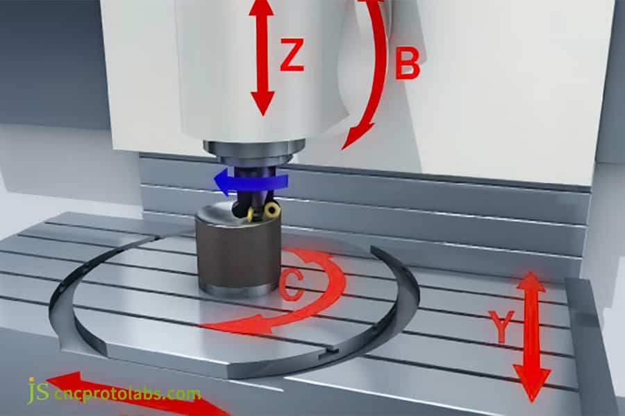
Figure 1 Five axis machining technology has unparalleled efficiency in processing complex geometric shapes.
How Does High Precision CNC Machining Ensure Semiconductor Components Are Fail-Safe?
High precision CNC machining is the key to ensuring zero fault operation of semiconductor components. The semiconductor industry relies greatly on component precision, particularly for better performance, thus, machine accuracy is dependent on quality aspects.
Defining High Precision: Typical CNC Machining Tolerances in the Semiconductor Field
It is characterized by the need of the components to have a very high level of tolerance. Various components require different precision indicators. The following table shows typical tolerance requirements for common semiconductor components:
| Part Type | Tolerance Requirement | Application Significance |
| Locating Pin Hole | ±0.005mm | Ensures precise part positioning and avoids assembly gaps. |
| Sealing Plane | <0.01mm/100mm | Ensures vacuum sealing and prevents particulate contamination. |
| Wafer Carrier | ±0.003mm | Maintains wafer flatness and ensures processing uniformity. |
| Reaction Chamber Inner Wall | <φ0.008mm | Ensures a uniform process environment and improves product quality. |
| Gas Nozzle | ±0.002mm | Controls gas flow rate and direction, stabilizing the process. |
These tolerance values are not arbitrarily set, but are determined based on the working principle and application environment of semiconductor equipment, and are also the core manifestation of CNC machining tolerances in the semiconductor field.
For example, the flatness of the sealing plane directly affects the vacuum holding capacity of the equipment. If it exceeds the limit, it may cause vacuum leakage, affecting the normal operation of the process. This also confirms the importance of precise control of CNC machining tolerances.
Building a Quality Fortress: Full-Process Inspection and Control
JS Precision sets up a triple control system for precision: online probes monitor and make real-time adjustments in parameters, accomplishing closed-loop control, finished products are all inspected using coordinate measuring machines and other equipment, key processes are completed in a cleanroom at 20±0.5 ℃ and 45% - 60% humidity to avoid environmental interference.
Precise Collaboration of Materials and Processes
Process optimization for different materials: The 6061-T6 aluminum alloy is annealed before machining to relieve stress. After the machining of 316L stainless steel, it will be passivated for corrosion protection, while PEEK materials can be cut at low temperatures to prevent deformation and reduce the defect from the source.
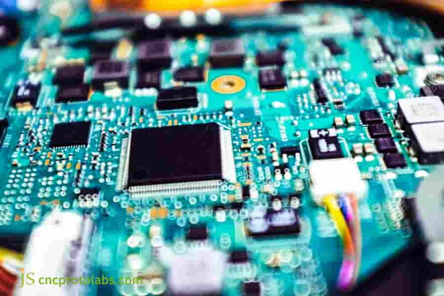
Figure 2 Semiconductor components are extremely small and typically require complex features and strict tolerance requirements.
Is Small Batch CNC Machining The Right Strategy For Semiconductor R&D And Production?
Characterized by the rapid pace of technological update and fluctuations of market demand, the semiconductor industry is a key area addressed by the efficient support of small batch CNC machining, which balances the factors of “efficient, cost-effective, and flexible,” playing a very vital role in the support of the industry.
Agile Path from Prototype to Verification
For small-batch production, it is possible to finish rapid prototyping and small-batch test production in 2-4 weeks. As a result, the speed in product R&D is shortened by 30%-50% using traditional large-scale production techniques, thus ensuring the rapid capture of the market share.
Reduced Inventory and Trial-and-Error Costs
No need for high mold investment, can be directly processed according to 3D models, avoiding mold scrap losses and inventory backlog, can reduce R&D trial and error costs by 40% -60%, and adapt to frequent design adjustments.
Seamless Integration with Mass Production: Process consistency
Through standardized programming, tooling, and process management, JS Precision directly reuses trial production parameters to carry out mass production, thereby guaranteeing quality and saving time.
| Comparison Metrics | Small Batch CNC Machining | Traditional Mass Production |
| Mold Investment | Zero investment | $10,000-$100,000 |
| Production Cycle | 2-4 weeks | 8-12 weeks |
| Trial and Error Cost | Low, flexible parameter adjustment | High, cumbersome mold modification |
| Inventory Pressure | On-demand production, low pressure | Requires stockpiling, high pressure |
| Applicable Scenarios | R&D prototypes, small batches | R&D prototypes, small batches. |
What Should You Look For In a Precision Machining Services Partner For Semiconductor Applications?
The selection of the right precision machining services provider is essential for semiconductor component manufacturing. High quality partners not only provide high-precision products, but also offer comprehensive support such as technical guidance and supply chain assurance.
Therefore, semiconductor component manufacturers should keep certain attributes in mind while selecting the right semiconductor CNC manufacturing service provider.
Experience Over Parameters: Deep Industry Knowledge
They should be skilled in the areas related to the requirements of the semiconductor equipment in terms of the particle size, the output rate of the gas, as well as the machinability of the materials used in the equipment, including the EFEM frame and the gas distribution disc, among other requirements.
A Visualized List of Capabilities and Qualifications
The key evaluation indicators include the company’s ownership of a clustering of CNC machines with at least five axes and precision machining capability, certification from the CNAS internal laboratory, SEMI S2/SEMI S8 certification, and the capability to support design-for-manufacturability.
A Reliable Supply Chain and Transparent Collaboration
Also, suppliers must ensure an on-time delivery rate of over 95%, have project engineers assigned to projects, and ensure a transparent communication pattern with customers from design recommendation to completion, so customers can monitor projects in real time.
If you are unsure how to choose a precision machining services partner, please note your core needs and contact us. JS Precision will provide a detailed supplier evaluation list and professional consultation to help you select the most suitable semiconductor component manufacturing partner.
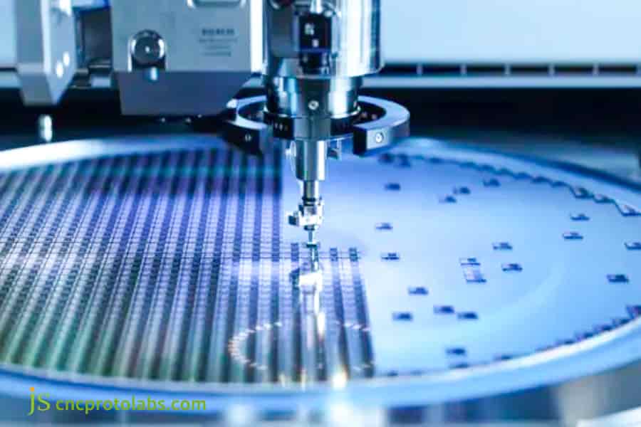
Figure 3 Modern precision machining utilizes computer-controlled equipment to manufacture complex parts, meeting the growing demands of the semiconductor industry.
How To Obtain An Accurate And Transparent Quote For Semiconductor Parts Machining?
Obtaining precise and transparent semiconductor parts machining quote is an important step in the procurement of semiconductor components. A reasonable quotation can help you control costs and avoid future cooperation disputes. To obtain a high-quality quotation, it is necessary to prepare in advance and interpret the quotation content correctly.
Essential Information for Quotations: Provide These Key Items
While making an application requesting a quote, you must provide detailed information, such as 3D/2D drawings and detailed tolerances, material requirements, material and/or certifications required, surface treatments and cleanliness required, quantity, delivery date, operational requirements, and special requirements, if applicable.
Cost Breakdown: Five Core Factors Driving Pricing
The semiconductor parts machining quote mainly consists of the following five parts:
| Cost Composition | Specific Content | Percentage of Total Quote |
| Material Costs | Cost of raw materials such as semiconductor-grade aluminum alloy sheets and special ceramics. | 20%-30% |
| Programming and Tooling Preparation Costs | Time cost of computer-aided manufacturing programming, tool design, and fixture fabrication. | 15%-20% |
| Machine Tool Occupancy Costs | Actual machining time cost of parts on CNC equipment. | 30%-40% |
| Secondary Processing Costs | Cost of subsequent processes such as surface treatment, cleaning, and heat treatment. | 10%-15% |
| Quality Inspection Costs | Cost of full-process inspection using high-precision instruments. | 5%-10% |
Gain Insight into Supplier Professionalism Through Quotations
A quotation from a professional reflects the strength and earnestness of their cooperation. Analyzing a quotation involves paying attention to the following aspects:
- Is it a detailed quotation (i.e., do all the items for costing appear separately)?
- Does it contain alternative processing suggestions for reducing costs?
- Do the quotations explicitly involve testing reports, quality commitments, and intellectual property confidentiality contracts?
Want an accurate semiconductor parts machining quote? Upload your part drawings and technical requirements. JS Precision will provide a detailed and transparent quotation within 3 business days, explaining the cost structure and processing solutions step by step.

Case Study: JS Precision Masters a 0.005mm Flatness Challenge On Semiconductor-Grade Ceramic
In the field of semiconductor CNC precision machining, the machining of high-precision ceramic parts is always considered to be a key technical problem. The successful machining project of ceramic electrostatic chuck (ESC) with very high flatness requirement by JS Precision entirely shows the strong capabilities of the company in high precision CNC machining.
Customer Challenge: Extreme Flatness Requirements for Ceramic Electrostatic Chucks
A leading semiconductor equipment manufacturer demands customized, alumina, ceramic, electrostatic, chucks for its emerging wafer fab tool platforms. Critical technical characteristics of the demand base are:
Flatness of the critical interface < 0.005mm, surface roughness < 0.1 microns, and no micro-cracks can be accommodated. Regular grinding process cannot meet flatness and surface integrity criteria simultaneously, and the customer has been consulted by several material suppliers.
JS Precision Solution: Combining Innovative Processes with Ultimate Control
Answering the needs of the client's difficulties, the engineering team at JS Precision developed a customized solution using the company's own processing technology:
1. Customized Process Development: Ultrasonic vibration-assisted five-axis precision milling technology replaced grinding processes. Customized cutting tools made of synthetic diamonds ensured high material removal rates while avoiding subsurface damage.
2. Environmental and Process Control: The entire processing was done in a temperature-controlled (20 ± 0.5℃) cleanroom. Online probes were used for error compensation in real-time, as well as stress relief treatment.
3. Multi-Dimensional Final Inspection: After processing, planar interferometry and a white light profilometer are utilized for final inspection with full area scans for conformance testing.
Quantitative Results: Outstanding Performance, Stable Delivery
For example, the level of flatness of the delivered item on the surface was 0.003mm, implying it had exceeded this measure by 40%. Additionally, the item’s surface had no traces of any micro-cracks. Besides these aspects, the project was completed within 8 weeks, implying it offered support in completing a new model for the customer.
Experience similar challenges in high-precision machining of semiconductor component parts? Contact JS Precision to see entire case details. Our engineers will provide a solution to your requirements with a high precision CNC machining solution to overcome your technology limitations.
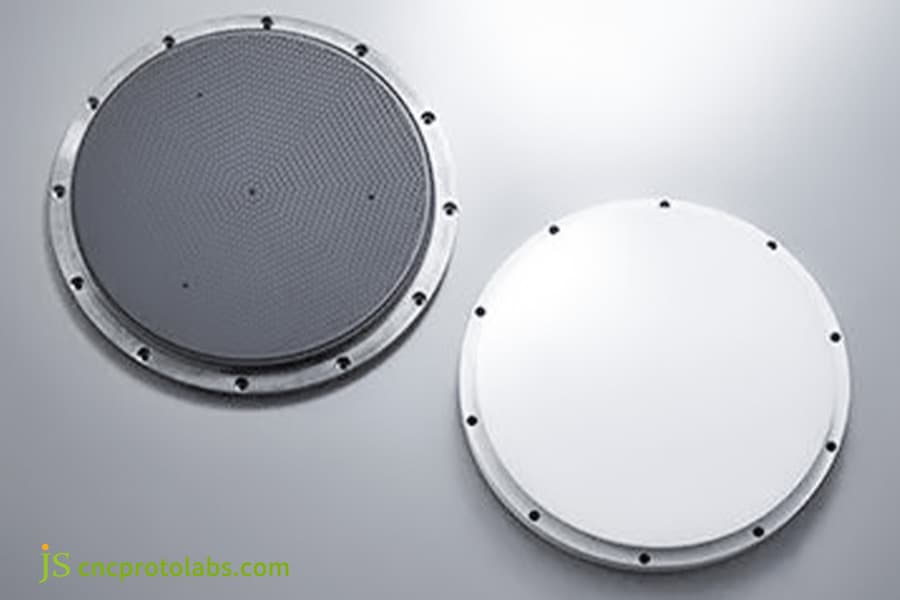
Figure 4 Aluminum oxide ceramic electrostatic suction cup
FAQs
Q1: What is semiconductor CNC precision machining? How does it differ from ordinary CNC machining?
Semiconductor CNC precision machining is a machining method designed specifically for semiconductor equipment parts. It performs far beyond the standards of ordinary industry in ultra precision machine tools, clean environments, special material processes, and sub micron level testing, ensuring ultra-high reliability of parts, which is difficult for ordinary CNC machining to achieve.
Q2: What commonly used semiconductor materials can JS Precision process?
It is possible to process a broad range of materials, including the important classes of wrought materials: Al-alloy grades 6061-T6, 5052, stainless steel 316L, 304, titanium alloy grades, nickel alloy grades, as well as advanced technical ceramic materials like alumina and aluminum nitride, in addition to important engineering plastics like PEEK, VESPEL, etc.
Q3: What's the smallest part you can process? What are the tolerance limits?
The least feature size of the part JS Precision can handle would be 0.1mm for micro-sized parts. The tolerance level of JS Precision would normally be ±0.005mm, however, JS Precision would accept tolerance limits of ±0.002mm.
Q4: How do you ensure cleanliness during processing and prevent particulate contamination?
JS Precision employs clean room techniques in several of its processes, using special tools and cutting fluids, then finishing methods such as ultrasonic cleaning and plasma cleaning that ensure the parts reach the required level of cleanliness, e.g., ISO Class 5, before they come out of the warehouse.
Q5: Do you provide surface treatment and post-processing services?
Yes, JS Precision offers one-stop service for anodizing, electroless nickel plating, electropolishing, and laser marking. Further, all the treatments are compliance to contamination prevention and corrosion resistance in the semiconductor industry.
Q6: How long does it usually take from inquiry to receiving samples?
JS Precision will make a detailed quotation within 3 working days once the data is received. It will take around 2~3 weeks for simple part samples, and approximately 4~6 weeks for complex samples.
Q7: Does the company support the transition from prototype to mass production?
Fully supported, one of the core advantages of JS Precision is to ensure that the process parameters and quality control standards validated during the prototype phase can be seamlessly transplanted into subsequent large-scale production.
Q8: What support is provided if problems are found during part assembly or testing?
JS Precision offers comprehensive after-sales technical service support. If there are accompanied problems related to manufacturing, we would focus on the process of investigation to find the solution.
Summary
In the ultimate pursuit of semiconductor manufacturing, the precision and reliability of components directly determine the performance boundary of equipment.
Semiconductor CNC precision machining is not simply processing incoming materials, but a system engineering that integrates cutting-edge equipment, profound process knowledge, and strict quality management.
JS Precision represents a choice of partner who can handle tolerances up to ±0.005mm, complex ceramic materials, and five-axis complex surfaces. Choosing JS Precision means choosing access to an extended engineering team that understands the industry and solves challenging problems.
Please send us your part drawing and technical requirements, the expert team at JS Precision will offer a tailor-made solution containing manufacturability analysis, transparent cost breakdown, and a workable delivery plan. Let's start building your demand for precision into the determining factor in your product's advantages in the marketplace.

Disclaimer
The contents of this page are for informational purposes only.JS Precision Services,there are no representations or warranties, express or implied, as to the accuracy, completeness or validity of the information. It should not be inferred that a third-party supplier or manufacturer will provide performance parameters, geometric tolerances, specific design characteristics, material quality and type or workmanship through the JS Precision Network. It's the buyer's responsibility Require parts quotation Identify specific requirements for these sections.Please contact us for more information.
JS Precision Team
JS Precision is an industry-leading company, focus on custom manufacturing solutions. We have over 20 years of experience with over 5,000 customers, and we focus on high precisionCNC machining,Sheet metal manufacturing,3D printing,Injection molding,Metal stamping,and other one-stop manufacturing services.
Our factory is equipped with over 100 state-of-the-art 5-axis machining centers, ISO 9001:2015 certified. We provide fast, efficient and high-quality manufacturing solutions to customers in more than 150 countries around the world. Whether it is small volume production or large-scale customization, we can meet your needs with the fastest delivery within 24 hours. Choose JS Precision this means selection efficiency, quality and professionalism.
To learn more, visit our website:www.cncprotolabs.com
Resource